





High-purity SiC ceramic components: a key material puzzle for the localization of semiconductor equipment
As the core functional components of semiconductor manufacturing equipment, high-purity silicon carbide ceramic components perform important functions such as bearing, protection, and diversion in key processes such as etching, thin film deposition, diffusion, and epitaxy. The high hardness, high thermal conductivity, low thermal expansion coefficient, and excellent plasma corrosion resistance of silicon carbide ceramics make them an ideal choice to meet the strict requirements of cleanliness and stability in advanced processes.
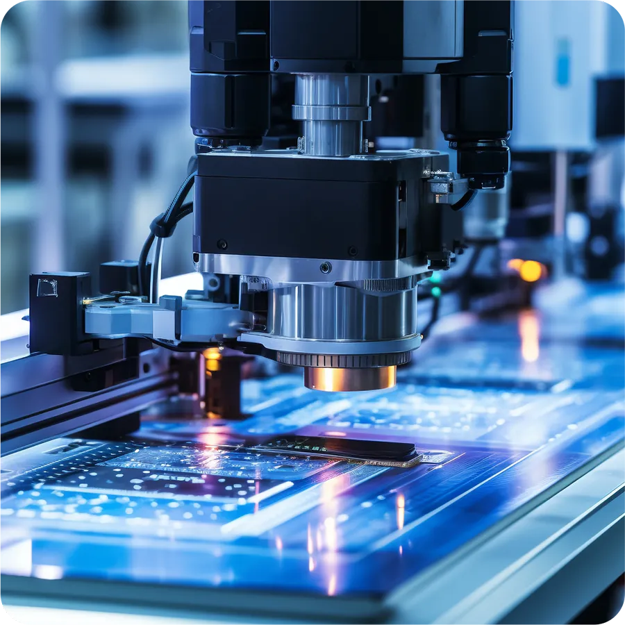
Silicon carbide ceramic components are mainly divided into two categories according to the preparation process: sintered silicon carbide and CVD silicon carbide. Sintered silicon carbide is suitable for large-size structural parts, while CVD silicon carbide has irreplaceable advantages in functional components such as etching rings and gas sprinklers due to its higher purity and density. In semiconductor manufacturing equipment, high-purity silicon carbide ceramic components are mainly used in scenes such as photolithography machine workpiece stages, etching equipment cavity liners, epitaxial equipment bearing bases, and wafer handling arms.
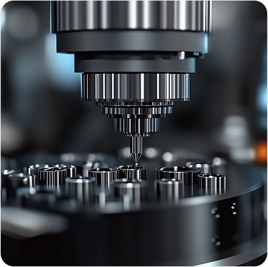
In terms of material system, the technical threshold of high-purity silicon carbide ceramic components is mainly reflected in three aspects: first, the stable supply of high-purity powder, high-end silicon carbide powder is still partially dependent on imports; second, the molding and sintering deformation control of large-size components, the shrinkage uniformity control of large-size components during the sintering process is the key to ensuring the yield; third, the precision machining ability, the dimensional accuracy and surface quality of complex structural components directly affect the performance of equipment, and high-precision grinding can reach micron-level dimensional tolerances and nano-level surface roughness.
From the perspective of industrial dynamics, the industrialization process of high-purity silicon carbide ceramic components is accelerating. The R & D and industrialization construction of silicon carbide ceramic parts aims to achieve large-scale mass production of silicon carbide ceramic parts through the construction of CVD-SiC ceramic parts production lines, and fill the industrial bottleneck of insufficient self-sufficiency of domestic high-end SiC ceramic parts. Large-size and complex shape pressureless sintered silicon carbide ceramics and high-purity coating processes for semiconductor equipment have successively entered the verification system of domestic mainstream equipment manufacturers and chip manufacturers. Some products have been delivered in small batches, and industrialization projects are expected to achieve large-scale output.
The analysis points out that with the continuous breakthroughs of domestic silicon carbide ceramic enterprises in material research and development, process equipment and product verification, the localization rate of high-purity silicon carbide ceramic components is expected to increase steadily, providing important support for the independent control of key components of semiconductor equipment.
Previous : CVD silicon carbide technology: high-performance solutions for semiconductor key components
Next : Preparation Process and Performance Advantages of CVD SiC Parts
 Return to previous page