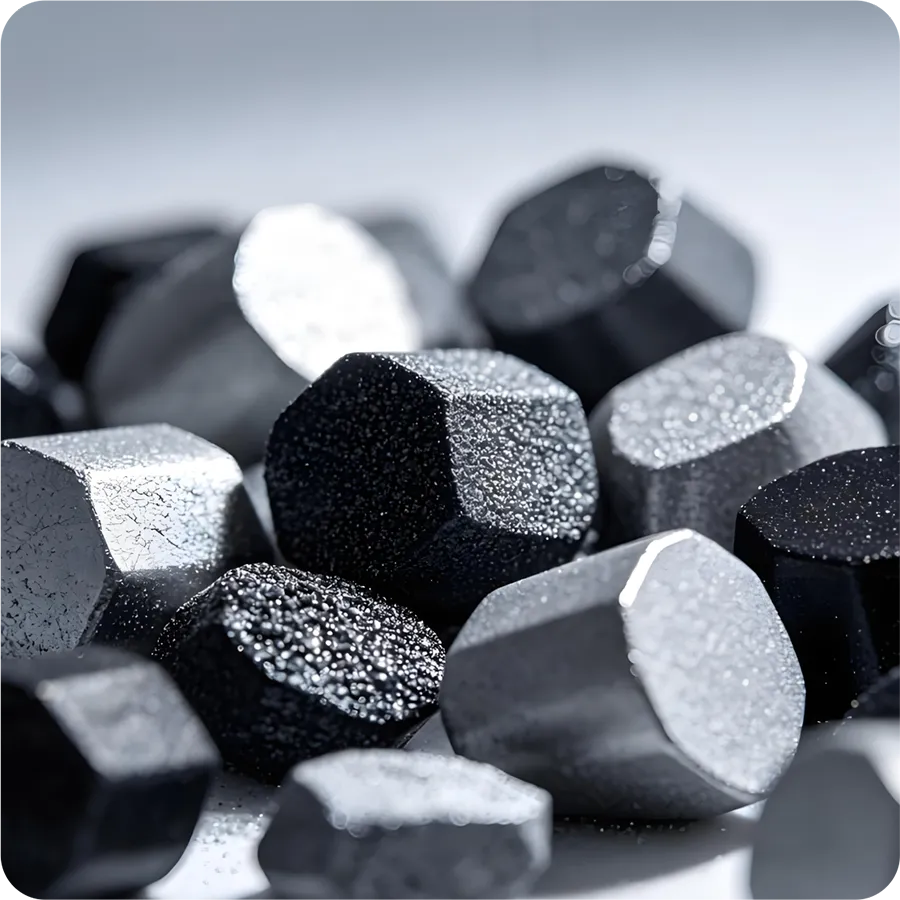






300Mm wafer fab equipment spending continues to grow, driving demand for semiconductor ceramic parts
According to SEMI's latest 300mm fab equipment spending forecast report, global 300mm fab equipment spending is expected to reach $133 billion in 2026, an increase of 18% year-on-year; it will further increase to $151 billion in 2027, an increase of 14% year-on-year. In the next three years (2026 to 2028), the total global 300mm fab equipment spending is expected to reach about $374 billion, providing important support for the semiconductor equipment and components market.
From the perspective of the global semiconductor ceramics and materials market, the global market size is about 2.867 billion US dollars in 2025, and it is expected to reach 4.518 billion US dollars in 2032, with a compound annual growth rate of 6.8%. Ceramic materials (including silicon carbide, alumina, aluminum nitride, etc.) have become indispensable key materials in semiconductor manufacturing equipment due to their high hardness, corrosion resistance, low thermal expansion coefficient and high insulation.
At the application level, semiconductor ceramic parts mainly cover key process equipment such as etching, thin film deposition, heat treatment, and ion implantation. Among them, silicon carbide ceramics are suitable for parts that require precise motion control such as lithography machine workpieces due to their high thermal conductivity and low thermal expansion coefficient; alumina ceramics are widely used in electrostatic chucks and etching cavity protection due to their good cost performance; aluminum nitride ceramics have advantages in electrostatic chucks and high-power heat dissipation components due to their excellent thermal conductivity.
From the competition landscape, Japanese companies hold a major share of the global semiconductor ceramics market, with the top eight global players accounting for about 83% of the market in 2024. Chinese companies have a market share of about 5.5% in this field, but it is growing rapidly. The size of China's semiconductor precision ceramics market in 2024 is about 165 million US dollars, and it is expected to reach 618 million US dollars in 2031, with a compound growth rate of about 18.58%.
The analysis points out that the future growth of semiconductor structural ceramics will focus on applications in more extreme process environments: advanced logic nodes, 3D NAND high-depth structures, and high-temperature, strong corrosion environments brought by compound semiconductors such as silicon carbide/gallium nitride, which place higher demands on the purity, consistency, and reliability of ceramic materials. At the same time, it also provides development space for enterprises with precision machining and material research and development capabilities.
Next :No.
 Return to previous page